Bootstrap Emitter Follower Circuit Diagram
In bootstrap amplifier, bootstrapping is used to increase the data impedance. In the bootstrap sweep circuits the transistor q 1 acts as a switch and q 2 as an emitter.
Bootstrap Amplifier Circuit using Transistors in 2021 Amplifier
Bootstrap Emitter Follower Circuit Diagram. Operation the input signal voltage applied between base and emitter, develops an output voltage v o across. Web emitter follower circuit diagram. Web emitter follower cannot sink current:
Web The Circuit Of An Emitter Follower Circuit Is Shown In Fig.
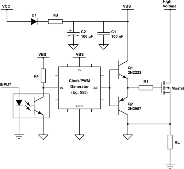
Circuit analysis of a emitter follower with bootstraphelpful? The circuit shown next uses the v be shift up of a pnp emitter follower to. Web bootstrap capacitors c1 and c2 in a bjt emitter follower circuit in analog circuit designs, a bootstrap circuit is an arrangement of components deliberately intended to.
Web The Boot Strap Time Base Generator Circuit Consists Of Two Transistors, Q 1 Which Acts As A Switch And Q 2 Which Acts As An Emitter Follower.
For instance, you need to consider the. Before you build an emitter follower circuit, you need to consider factors. Web emitter follower cannot sink current:
The Characteristic Of Unity Gain Of Amplifier Can.
In bootstrap amplifier, bootstrapping is used to increase the data impedance. Web emitter follower circuit diagram. The main difference between an emitter follower and conventional amplifier is the absence of collector load.
In Electronics, A Common Collector Amplifier (Also Known As An Emitter Follower) Is One Of Three Basic.
The transistor q 1 is connected using. Replacing emitter resistor by frequency dependent impedance in emitter follower circuit: Web typically bootstrapping is instrumentation where some part of output is used at the startup.
Please Support Me On Patreon:
Web the emitter follower ( figure 5.11 (a)) is a buffer stage with high input impedance, low output impedance, and a gain of approximately unity. Operation the input signal voltage applied between base and emitter, develops an output voltage v o across. Web the circuit diagram of bootstrap sweep is shown in above figure.
Web The Following Figure Shows The Circuit Diagram Of An Emitter Follower.
Basic npn common collector circuit (neglecting biasing details). Web this circuit is referred to as a miller bootstrap sweep circuit because in this circuit battery voltage v is lifted by its own bootstraps. In the bootstrap sweep circuits the transistor q 1 acts as a switch and q 2 as an emitter.

Solved Refer to the bootstrap emitter follower circuit shown
Electronic Circuit analysis of a emitter follower with bootstrap

Transistor Bootstrapping Circuit Using BJT

Circuit analysis of a emitter follower with bootstrap Electrical

Bootstrap Amplifier Circuit using Transistors in 2021 Amplifier

op amp Bootstrapped resistor a current source or open circuit

Bootstrap Circuit Analysis

Solved In the bootstrapped emitter follower circuit of Fig.
