Bcd Adder Subtractor Circuit Diagram
Web the bcd adder subtractor circuit diagram is composed of several components. Each of the decimal digits can be coded in binary using four bits.
bcd subtractor circuit diagram Wiring View and Schematics Diagram
Bcd Adder Subtractor Circuit Diagram. Web block diagram of combinational logic circuit: 4.21 and the 9’scomplementer of problem 4.18. Web a bcd adder is a circuit that adds two bcd digits in parallel and makes a sum digit also in bcd.
Use Block Diagrams For The Components.
Output depends upon the combination of inputs. Representation is called binary coded decimal or bcd. The digital systems handles the decimal number in the form of binary coded decimal numbers.
Web Download Scientific Diagram | Bcd Detection And Correction Circuit From Publication:
Web the bcd subtractor circuit is an incredibly versatile and efficient way to perform digital subtraction. Web this problem has been solved! Use the bcd adder of fig.
Web A Bcd Adder Is A Circuit That Adds Two Bcd Digits In Parallel And Makes A Sum Digit Also In Bcd.
So far i have managed to draw out the full binary adders will xors on the b inputs for a 1's. You'll get a detailed solution from a subject matter expert that helps you learn core concepts. Web the bcd adder subtractor circuit diagram is composed of several components.
Each Of The Decimal Digits Can Be Coded In Binary Using Four Bits.
Web and optimize proper circuits for a reversible bcd adder/subtractor such as full adder, re versible 9’s complement generator and reversible multiplexer. The first component is the adder, which consists of two or more gates. 1 shows the conventional bcd adder.
It Features An Ic 7483 Circuit Diagram, Which Is A.
Web download scientific diagram | an irreversible bcd adder from publication: Web bcd adder is a circuit that adds two bcd digits in parallel and produces a sum digit also in bcd. Web block diagram of combinational logic circuit:
Design And Optimization Of Reversible Bcd Adder/Subtractor Circuit For Quantum And.
A bcd adder must also include the. Points to remember on combinational logic circuit: A bcd adder should contain the correction logic in its internal.
[Block Diagram Of The Bcd Adder Has 9 Inputs (Two Bcd Digits And A Carry In) And 5.
A unified reversible design of binary and binary coded decimal adder / subtractor |. Web needed to add or subtract decimal numbers. 4.21 and the 9’scomplementer of problem 4.18.
Web Bcd Adder Circuit | Bcd Adder Truth Table | Bcd Adder Block Diagram:
4.19 construct a bcd adder. Web it has to add 2 bcd numbers together and have a carry in and out. Web overview test series with this article on adders, we will be starting our discussion with a combinational circuit and will answer all the questions regarding.

Solved Construct a BCD addersubtractor circuit. Use the BCD a

bcd subtractor circuit diagram Wiring View and Schematics Diagram

FPGA implementation of the adder stage for a 10’s complement BCD

Block Diagram of BCD Adder Download Scientific Diagram
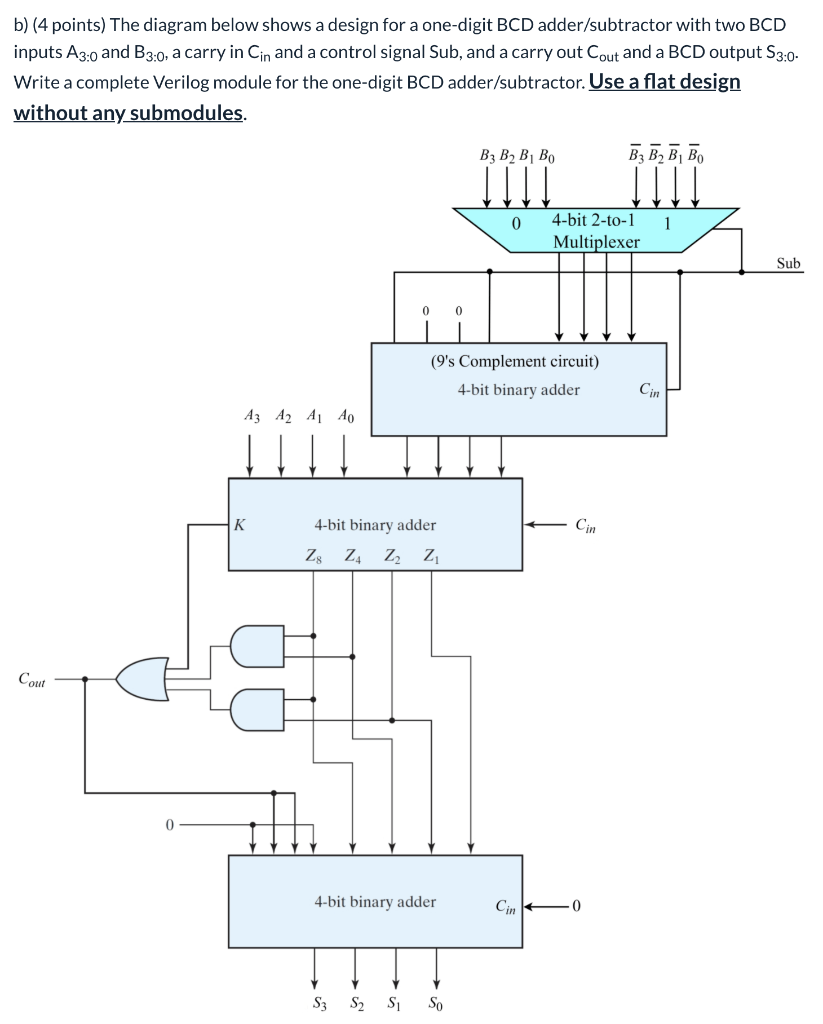
Solved b) (4 points) The diagram below shows a design for a

Proposed 1Digit BCD Adder Circuit. Download Scientific Diagram

bcd subtractor circuit diagram Wiring View and Schematics Diagram

Proposed binary/BCD adder/subtractor Download Scientific Diagram
